Perovskite solar cells are an important research direction emerging in the field of photovoltaics in recent years. Due to its excellent self-assembly characteristics, organic-inorganic hybrid perovskites can realize large-area solar cell module preparation, rich and cheap raw materials and rapid development of device efficiency through simple low-temperature wet process, making it commercial in the future It shows great potential in applications. However, the current mainstream device structure generally uses n-type semiconductor materials prepared at high temperature such as TiO2 as the electron transport layer, which increases the manufacturing energy consumption and cost of the device, and limits the construction of flexible devices. Moreover, the strong UV photocatalytic performance of metal oxides such as TiO2 is an important reason for the poor light stability of the device. Therefore, it is very important to avoid the use of such transmission materials or develop new interface modification materials.
Recently, Ge Ziyi's research group of Ningbo Institute of Materials Technology and Engineering, Chinese Academy of Sciences has made a series of research progress on this issue.
First, based on the results of previous studies (ACS Applied Material and Interfaces 2016, 8, 9811-9820, Solar Energy Materials & Solar Cells 2016, 157, 1038-1047), the introduction of external dopants to control the perovskite carriers Type, which is used to synergistically optimize the band structure and energy level alignment of the front and back interfaces of the perovskite absorber layer, and construct a pn heterojunction prototype device with high efficiency rectification characteristics. The performance of similar devices provides a new idea (Figure 1). Related results were published in Solar RRL (DOI: 10.1002 / solr.201800274).
Further, in response to the problems in the development of such devices, the researchers made an in-depth and comprehensive literature review, and the relevant results were published in Advanced Energy Materials (2019, 1900248). Based on these new insights, the researchers innovatively used the small molecule interface material MSAPBS developed in the early stage of the research group for transparent conductive glass (TCO ) Work function control and passivation of interface defects in front of the device (Figure 2). The introduction of the interface material significantly reduces the work function of TCO and the electron collection barrier of the perovskite / TCO interface. The optimized interface band bending achieves efficient electron selective collection; the SO3- and NH3 + in the molecules of the interface layer There is a defect state that further passivates the perovskite / TCO interface, ensuring efficient electron collection, while at the same time significantly improving the short-circuit current density, open circuit voltage, and fill factor of the device, and finally achieving a metal-free efficiency of 20.6% Oxide electron transport layer perovskite solar cell. Since the elimination of the electron collection barrier and the passivation of interface defects suppress the charge accumulation, the hysteresis effect of the device is suppressed, and the stability is also significantly improved. Related research work was submitted to Advanced Science (2019, DOI: 10.1002 / advs.201902656).
In addition, through the cooperation with Tobin J. Marks and Antonio Facchetti's group of Northwestern University professors, this type of interface material was introduced into the classic planar heterojunction structure perovskite solar cell, and the front interface of the device was passivated from the bottom The bulk defect state of the perovskite absorber layer suppresses the hysteresis effect of the device, and significantly improves the photoelectric conversion efficiency (21.18%), environmental humidity and heat stability, and light stability of the device (Figure 3). Related research work was published in Advanced Materials (2019, 1903239).
The above research was supported by the National Natural Science Foundation of China (61904182), the Postdoctoral Research and Innovation Talent Support Program (BX20180322), the National Key R & D Program (2016YFB0401000), the Zhejiang Provincial Outstanding Youth Fund (LR16B040002), the Ningbo Science and Technology Innovation Team (2015B11002, 2016B10005), the Chinese Academy of Sciences Funded by key research projects in frontier science (QYZDB-SSW-SYS030), key international cooperation projects of the Chinese Academy of Sciences (174433KYSB20160065) and the National Natural Science Foundation Outstanding Youth Fund (21925506).

Figure 1 (a, b) UPS spectrum of the perovskite thin film before and after doping, the energy level alignment change of each functional layer of the device (c), before (d) and after doping (e) device band structure Variety

Figure 2 (a) SEM photo of device cross-section, (b) device energy band structure, comparison of device performance parameters of reference group and optimized group: JV curve (c), EQE curve (d), steady-state output curve (e) and performance parameters Statistical distribution (f)
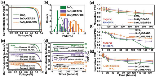
Fig. 3 (a) JV curve of the optimal device with different electron transport layers, statistical distribution of device performance parameters (b), hysteresis characteristics of the device (c), steady-state output of the device (d), and thermal stability test of the device (e, f) and light stability test (g)
Automatic Door Operator,Dorma Automatic Door Operator,Door Sensor Operator,Automatic Door Opener Operator
Caesar door control co.,ltd , https://www.caesar-door.com